Solutions
Advanced High-Technology PCBs
Day in and day out, we manufacture the most advanced high-technology PCBs that incorporate the most complex features in the PCB industry. We work with our customers at the very early stages of their product development to help them design a PCB that is both robust in features as well as being manufacturable. Having invested significantly in people, processes, and equipment, we have the technical know-how to ensure that we can deliver the most advanced PCBs with consistent quality and on schedule.
To ensure quality, all panels contain reliability coupons per IPC-2221 that are used for both in process and final inspection criteria. We can meet IPC Class III, MIL-STD-31032, and AS9100 requirements on any technology that we produce as we have all of the in-house laboratory and automated inspection equipment to ensure compliance. Many companies today try to focus and invest on being both a PCB fabricator and PCB assembler. Our strategy is to focus on being a world class leader in PCB fabrication and put all of our resources toward that single goal.
See our blog post on IPC Class III vs. MIL Spec for Printed Circuit Boards for more information.
Services
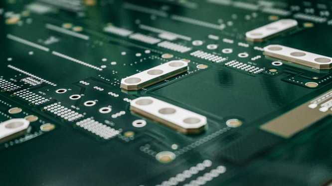
- Rigid PCBs up to 40 layers
- Quick-turns and Standard Delivery
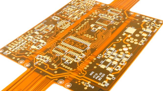
- Flex and Rigid-Flex PCBs
- Heavy Copper PCBs
- Embedded Resistors
- PCB Design Services
- Inventory Management
- Specialty RF & Microwave PCB
- Advanced HDI Circuit Boards
- Back Planes and Probe Cards
Our Parent Company, Epec Engineered Technologies is the ideal choice for an OEM seeking customized product solutions from a focused and agile partner having supported over 5,000 customers across all sectors of the electronics industry. By providing highly experienced technical resources, a proven manufacturing platform and the fastest delivery in the industry, we are able to provide cost effective and innovative solutions that deliver the highest reliability products to the market faster.
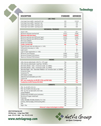
Technology
- Blind and/or buried vias, which account for approximately 40% of our work
- Conductive and non-conductive filled vias (i.e., VIP or via-in-pad technology), which accounts for better than 50% of the part numbers we build
- 100% Plated Filled Vias – specialized process
- Ultra-High Aspect Ratio (> 34:1)
- Controlled depth pockets, both plated and non-plated for various mechanical requirements
- Mixed package designs, where we bond and process different materials together
- Expertise in edge plating and castellation holes through a well-developed process
- Etched resistors on 25, 50, 100, and 250 ohms per square (Ticer and OhmegaPly)
- Electroless Nickel/Electroless Palladium/Immersion Gold (ENEPIG), in-house and regarded as the most superior surface finish available; also compatible with wire bond applications
- Microvias down to 0.004”, including 1+N+1, 2+N+2 and 3+N+3 stacked and/or staggered construction
- Copper and aluminum bonded boards for heavy thermal dissipation
- Electroplated nickel, palladium, and gold finishes available for oil & gas applications requiring high reliability in harsh environments
Materials
- Rogers RO4350, RO4003, RO6035HTC, RO6002, RO3006, TMM and 2929 bondply material fabrication for RF applications
- Taconic RF-35, TLX/TLY, TSM-DS3b and Fastrise for RF applications
- Arlon DiClad, CuClad and CLTE for RF applications
- Panasonic Megtron 6 & 7
- Isola I-Terra, Tachyon, I Speed for RF/Microwave Low Loss applications
- Isola 185HR, 370HR and FR408HR for enhanced FR4 applications, including RoHS compliant as well as lower loss
- Polyimide multilayers for military, aerospace, and the oil and gas industries – Isola P95/P25, Arlon 85N/85HP/86HP, and DuPont Pyralux
If you would like more information about some of the common materials we use, we suggest you visit these websites:
- Arlon (substrates)
- Isola (substrates)
- Rogers (substrates)
- Taconic (substrates)
- Ticer Technologies (resistive materials)
- Ohmega Technologies (resistive materials)
Tachyon® 100G for RF and High-Speed PCB Applications
Tachyon® 100G is a premium ultra-low-loss laminate system engineered for the most demanding RF, microwave, and high-speed digital designs. Its tightly controlled dielectric constant (around 3.02) and exceptionally low dissipation factor (about 0.0021) ensure outstanding electrical performance, with stability from –55°C to +125°C and frequencies up to 100 GHz. These characteristics make it ideal for applications requiring consistent impedance, minimal insertion loss, and reliable signal integrity across wide bandwidths.
At NetVia Group, we have manufactured over 500 unique PCB designs using Tachyon 100G. Our Dallas-based facility is equipped with advanced process controls, cleanroom handling, and RF-specific inspection capabilities required to build these boards to exacting standards. This experience allows us to deliver exceptional performance and repeatability for customers across aerospace, defense, telecommunications, and advanced networking sectors.
Why RF Engineers Choose Tachyon 100G
- Ultra-low loss and stable Dk/Df: With a dielectric constant near 3.02 and dissipation factor around 0.0021, Tachyon 100G minimizes insertion loss and provides consistent phase response across RF bands.
- Performance through 100 GHz:Its stable dielectric behavior across frequency and temperature supports mmWave, radar, and phased-array designs that depend on predictable electrical properties.
- Weave and copper options: Spread-glass and square-weave constructions reduce differential skews, while HVLP and VLP copper minimize conductor loss at microwave frequencies.
- Excellent thermal reliability: With a glass transition temperature near 215–230°C and low Z-axis expansion, Tachyon 100G endures multiple lamination cycles without reliability degradation.
- Manufacturing resilience: The resin system is CAF-resistant, exhibits very low moisture absorption, and integrates well into HDI and hybrid stack-ups.
Typical Applications
NetVia Group’s RF team regularly builds Tachyon 100G boards for:
- RF amplifiers, LNAs, and converter modules
- mmWave phased-array antenna tiles and beamforming subassemblies
- SATCOM and radar backplanes combining RF and high-speed digital circuits
- High-frequency clock and LO distribution networks requiring precise phase alignment
What Sets NetVia Group Apart
- Stack-up Design Expertise: Our engineering team collaborates with customers to design optimized core and prepreg configurations, manage copper roughness and glass weave orientation, and combine Tachyon with other laminates when hybrid builds are required.
- Process Control for RF Precision: We utilize tuned lamination profiles, alternative oxide treatments, and refined imaging processes to minimize loss and maintain impedance accuracy for high-frequency lines.
- Reliability and Verification: Our RF coupon testing includes insertion loss, return loss, and phase stability verification. Each build benefits from proven lamination recipes for multi-cycle HDI and high-layer-count reliability.
Quick Material Snapshot
- Dielectric Constant (Dk): ~3.02 at 5–10 GHz
- Dissipation Factor (Df): ~0.0021 at 5–10 GHz
- Thermal Properties: Tg ~215–230°C, Td ~360°C
- Copper Options: HVLP, VLP, and advanced RTF
- Moisture Absorption: ~0.1%
- Temperature Range: –55°C to +125°C
- Frequency Range: Stable up to 100 GHz
Partner with NetVia Group
Whether you need ultra-low-loss performance for X-, Ku-, or Ka-band RF systems or a hybrid board combining RF and high-speed digital, NetVia Group’s experience with over 500 Tachyon 100G builds ensures a process-proven path to success.
Talk to our RF engineering team to discuss your next design, review stack-up options, and plan a build that meets your performance, reliability, and production requirements.
Industries Served
- Defense & Aerospace
- Telecommunications
- Semiconductor
- Industrial
- Contract Manufacturing
- Medical
- Automotive
- Commercial


