HDI PCB Design Guidelines and Considerations
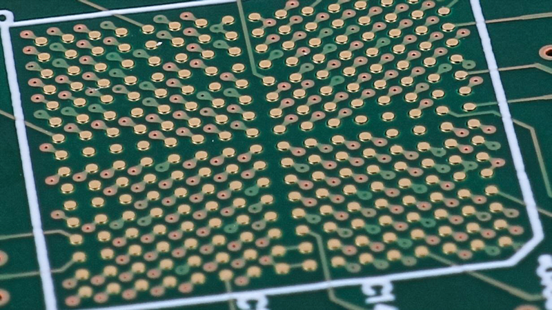
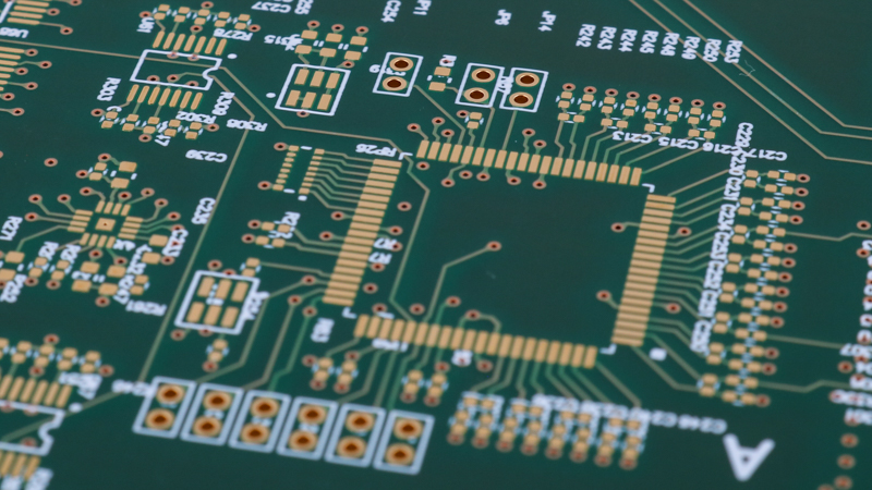
High-Density Interconnect (HDI) printed circuit boards (PCB) have a much higher circuit density compared to standard PCBs, which means more components can be placed on a smaller area. This is achieved by reducing trace widths, increasing layer counts, adding stacked/staggered/blind/buried vias, and using finer lines and spaces.
They are typically more expensive than standard PCBs due to the more complex manufacturing process and the use of specialized materials. The following are some key design considerations that need to be understood by the PCB designer as they need to be confident that their PCB fabricator understands the challenges around the high-technology circuit boards.


IPC-2226 Specification
In the IPC-2226 specification, HDI features are classified into three types:
- Type I: Microvia features, with a size of 0.15 mm (6 mils) or less.
- Type II: Blind via features, where the via does not pass through the entire board and terminates on an internal layer. The size of Type II vias is typically between 0.15 mm and 0.50 mm (6 mils to 20 mils).
- Type III: Through-hole via features, where the via passes through the entire board and extends out through both sides. The size of Type III vias is typically greater than 0.50 mm (20 mils).
Each type of HDI feature is designed to meet specific requirements and is used in different applications. The IPC-2226 specification provides design guidelines and performance criteria for HDI features and is widely used in the electronics industry as a reference for the design and manufacture of high-density printed circuit boards.
HDI PCB Stack-Up Requirements
HDI PCBs have specific stack-up requirements to meet the demands of high-speed signals, fine line and spacing capabilities, and reduced circuit size. The following are some of the key requirements for an HDI circuit board stack-up.
Layer Count
HDI circuit boards usually have more layers than traditional printed circuit boards, usually between 4 to 16 layers, allowing for more interconnections and higher circuit density.
Core Material
The core material is usually a low-loss substrate material, such as FR-4, or a high-performance composite material, such as PI (polyimide). The core material should have low dielectric loss and high thermal stability to support high-speed signals.
IPC-4101 slash sheet is a specification developed by the International Electronics Manufacturing Initiative (IPC) that defines the requirements for the laminate material used in printed circuit boards (PCBs). The slash sheet is a reference document that outlines the material properties and requirements for specific laminate grades and finishes.
It is used by PCB manufacturers and designers to ensure that the material used in the PCB meets the required specifications for electrical and mechanical performance. The IPC-4101 slash sheet is updated periodically to reflect changes in technology and advancements in materials.
Prepreg Thickness
Prepreg thickness is the material used between the core and the outer layers to ensure uniform layer thickness. HDI boards require precise control of the prepreg thickness to maintain high signal integrity and impedance control.
Lamination Technique
HDI circuit boards require precise lamination techniques, such as double-sided copper and copper-clad lamination, to achieve consistent layer thickness, low warpage, and high adhesion.
Impedance Control
Impedance control is critical in HDI circuit boards as it affects the performance of high-speed signals. The stack-up should be designed to provide consistent impedance values throughout the board.
Thermal Management
HDI circuit boards generate more heat due to the high density of components, so the stack-up should be designed to manage heat dissipation effectively. This can be done by using thermal vias or through-hole plating.
What is 1+N+1?
1+N+1 in PCB manufacturing refers to a stack-up structure in the design of a printed circuit board. The numbers 1 and 1 represent the number of copper layers (or other materials) in the core of the board, which provides the electrical connection and stability for the components. The "N" refers to the number of additional signal layers that can be added between the core layer. The value of "N” is determined by the complexity and number of electrical connections needed on the PCB.
For example, the term "4+n+4” in the sequential lamination of printed circuit boards refers to the number of layers used in the manufacturing process of a PCB.
The stack-up structure is crucial in determining the overall electrical performance, signal integrity, and thermal management of the PCB. By having 4 layers in the core and additional N layers in the inner portion, the designer can optimize the routing, shielding, and decoupling strategies to meet the electrical requirements of the board. The additional 4 layers in the core provide additional stability and improve the mechanical integrity of the board.
Overall, the 4+N+4 stack-up structure in PCB manufacturing provides a balanced design that offers the necessary electrical performance, reliability, and mechanical strength for the printed circuit board.
Sequential/Multiple Lamination Cycles
Sequential lamination of PCBs is a process where multiple layers of metal and insulating materials are stacked and laminated together in a sequential manner. This process is used to build multi-layer PCBs that have more complex and dense circuit layouts. In sequential lamination, each layer is added one by one, with a dry film photoresist material being applied on top of each layer and then etched to form the desired pattern. This process is repeated for each layer, and after all the layers are assembled, the entire stack is pressed and cured under heat and pressure to form a solid and highly dense PCB.
Each lamination cycle or a sequential lamination process involves stacking the desired number of layers of material, followed by the application of heat and pressure to bond the layers together. The process is repeated for each cycle until the desired final thickness is achieved.
Challenges Faced in Multiple Lamination Cycles In Printed Circuit Boards:
- Lamination Consistency: Ensuring consistent lamination quality across multiple cycles is a major challenge, as it is difficult to control the uniformity of pressure, temperature, and time, leading to uneven lamination.
- Delamination: Delamination is a common issue that occurs when the bond between the layers of a printed circuit board weakens or fails. This can occur due to multiple lamination cycles, which increase the risk of delamination and can result in the circuit board failing.
- Warping: Warping is another common problem associated with multiple lamination cycles. Warping occurs when the printed circuit board is not evenly heated and cooled, leading to distortion of the circuit board and causing it to become warped.
- Lamination Defects: Lamination defects, such as air bubbles, cracks, and voids, can occur during the lamination process. These defects can weaken the circuit board and reduce its reliability.
- Material Compression: Multiple lamination cycles can also result in material compression, which can cause the printed circuit board to lose its original thickness. This can impact the performance and reliability of the board.
Filled Vias
Filled vias in PCBs are vias that have been filled with a conductive material such as copper. A via is a small hole in a PCB that connects one layer of the circuit board to another. Filling vias with a conductive material helps to improve the electrical performance of the circuit board, as well as making the vias stronger and more reliable.
Two Main Types of Filled Vias:
- Copper-filled vias
- Conductive polymer-filled vias.
Copper-filled vias are the most common and are made by first drilling the via hole and then electroplating it with copper to fill the hole. Conductive polymer-filled vias are filled with a conductive polymer material, which provides good electrical performance and is also more cost-effective than copper-filled vias. To properly fill the vias with a conductive paste, specialized equipment with a vacuum that assures that the material is uniformly drawn through the hole is critical for high-quality filled vias.
The use of filled vias in PCBs is becoming more common, as they offer several benefits over unfilled vias, such as improved electrical performance, better heat dissipation, and increased reliability. However, they can also be more difficult to manufacture and more expensive than unfilled vias, so their use is usually limited to high-performance or high-reliability applications.

