Commercial HDI Printed Circuit Boards
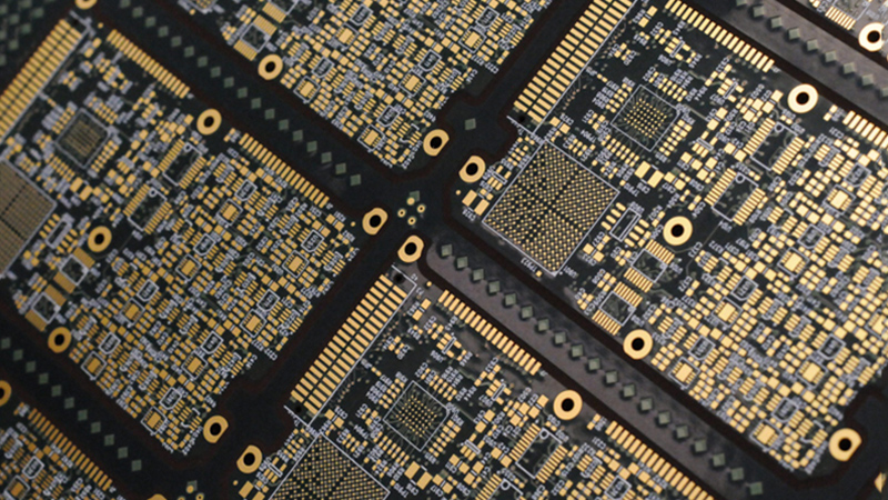
Commercial High-Density Interconnect (HDI) Printed Circuit Boards (PCBs) are circuit boards with a high component density, high layer counts, and fine line features, making them ideal for compact and high-performance electronic devices used in commercial applications.
Common Features of an HDI Printed Circuit Board
There are several key features of a circuit board that separates a circuit board from an HDI. These examples include but are not limited to:
- Fine Lines and Spaces
- High-Density Vias
- Microvias
- Increased PCB Layer Count
- Stacked Microvia Technology
- Blind and Buried Vias


Fine Lines and Spaces
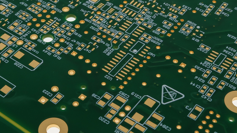
HDI boards have finer lines and spaces than traditional PCBs, allowing for higher component density. Fine lines and spaces in HDI printed circuit boards refer to the small dimensions of the conductive traces and the gaps between them on the board.
These PCBs with fine lines and spaces are an essential feature of HDI technology, as they allow for a higher component density on the board (the lines are of copper that is chemically etched off of the panel and can be as small as 2.5 mils in width). The fine lines and spaces allow for a higher number of components and interconnections in a given area, which leads to improved performance and a more compact design in electronic devices.
High-Density PCB Vias
Vias are tiny holes in the PCB that connect different layers, and HDI boards have vias with smaller diameters, enabling a higher number of vias per unit area. High-density vias (HDV) in HDI printed circuit boards refer to small vias with a diameter of 0.15mm or less that are used to route signals between layers of a PCB. These small vias are used in HDI PCBs to increase the density of the interconnections, allowing for more complex designs, higher component densities, and improved signal routing performance.
High-density vias are created using laser drilling, which precisely drills small vias with high aspect ratios (the ratio of the via's height to its diameter). This technology enables the creation of fine pitch vias, which can be positioned very close to one another, allowing for high interconnect density.
Microvias
Microvias are even smaller vias used to interconnect internal layers, further increasing the component density. Microvias in HDI-printed circuit boards are tiny electrical connections that run between the different layers of a circuit board. These small vias are used to increase the density and complexity of the circuits, allowing for more compact and efficient designs.
Micro vias are typically created using laser drilling technology, which allows for the precise and accurate formation of the vias, even in high-density interconnect circuit boards. The small size of micro vias enables a higher number of interconnections to be made in a smaller area, making them an essential component of high-performance printed circuit boards.
Increased PCB Layer Count
HDI circuit boards often have more layers than traditional PCBs, allowing for more routing space and increased performance. Like many of the features associated with HDI circuit boards, higher layer counts allow for more complex designs and more components to be integrated into a smaller space. This results in increased functionality and performance as with more layers, high-speed signals can be routed more efficiently, reducing crosstalk and improving signal integrity.
Along with that, higher layer counts allow for more redundancy and better thermal management, reducing the risk of thermal stress and increasing the overall reliability of the circuit board.
Stacked Microvia Technology
This is a technique used to connect internal layers by stacking microvias on top of each other, allowing for even higher component density. Stacked micro vias in HDI PCBs are multiple small vias that are stacked on top of each other to create a connection between multiple layers of the PCB. They are used to improve the density and functionality of the PCB and reduce the board size, making it possible to add more components and circuits in a smaller area.
Stacked microvias are laser drilled and plated, then laminated to the layer below it until the optimal number of PCB layers is complete. This is a very specialized technology that not very many fabricators have the capability of producing a reliable finished PCB.
Blind and Buried Vias
Blind and buried vias reduce the number of vias that pass through the entire board, reducing crosstalk and reducing the number of parasitic inductances and capacitances that affect signal integrity. Along with that, by reducing the number of vias in the board, blind and buried vias help to dissipate heat more effectively, reducing the risk of thermal damage to the components.
Blind and buried vias are typically manufactured using laser drilling, which results in more accurate and consistently drilled holes compared to traditional mechanical drilling methods.
Complexity of HDI Circuit Boards
Because of the complexity of HDI circuit boards, PCB fabricators must make a significant investment in equipment and have experience in engineering, production, laboratory, process control, and test.
Manufacturing Challenges When Making HDI PCBs:
- Complex Circuit Designs: HDI circuit boards have smaller and finer trace patterns, requiring advanced laser drilling and laser direct imaging techniques, leading to a higher degree of manufacturing complexity.
- High Aspect Ratios: The aspect ratio (the height of the hole divided by its diameter) is much higher in HDI circuit boards compared to traditional printed circuit boards, requiring advanced drilling and plating techniques to achieve accurate results.
- Limited Drilling Options: The small size of the vias and high density of the boards limit the number of drilling options available to manufacturers.
- Poor Copper Adhesion: Copper adhesion to the core substrate material can be challenging, especially when drilling small vias. This can lead to copper peel and breakage, making the circuit board unreliable.
- Testing Challenges: Testing and inspection of HDI circuit boards are more challenging due to the high density of the PCB, making it difficult to identify defects and malfunctions.
- High Cost of Manufacturing: The advanced techniques required for manufacturing HDI circuit boards, such as laser drilling and laser direct imaging, are expensive due to the cost of the equipment, making the PCB more costly to produce compared to traditional printed circuit boards.
- Material Selection: Selecting the right core substrate and material for the board is critical in HDI board manufacturing, as the material must have the necessary strength, thermal stability, and dimensional stability to withstand the high-density manufacturing process.
HDI-printed circuit boards for commercial applications have been a specialty of Netvia Group for many years. Being a key supplier for military and aerospace applications has allowed us to develop all of the key processes to ensure that our customers get the highest quality HDI circuit boards.

