PCB Back Drilling
Back drilling is a technique used in high-tech printed circuit boards (PCBs) to remove excess via stubs or portions of plated through-holes that extend beyond the intended signal layer. The primary reason for using back drilling is to improve the signal integrity of high-speed or high-frequency signals on the PCB.
When a signal passes through a via or plated through-hole, it can reflect back and cause unwanted noise or interference. This effect becomes more significant as the signal frequency increases, and the length of the via or hole becomes a larger fraction of the signal wavelength. By removing the excess via stubs or portions of plated through-holes, the signal's path is shortened, which reduces the reflection and the potential for noise or interference which is why back drilling is commonly used in high-speed digital designs and RF circuits.
How Back Drilling Is Done on A Circuit Board
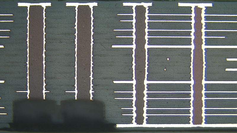
Back drilling is typically performed using a drilling machine that drills from the opposite side of the PCB to remove the undesired material. The drilled holes are typically larger in diameter than the original via or plated through-hole, which helps to prevent crosstalk or coupling between adjacent traces as it removes the portion of the via that extends beyond the layer that it connects to, effectively shortening the via and reducing its capacitance.
This reduces signal reflections, which can cause data errors and reduce signal quality. The depth of the drilled hole is usually calculated based on the specific design requirements, and the hole is typically filled with epoxy material to prevent solder wicking and provide stability to the via.
PCB Back Drilling on Multiple Layers
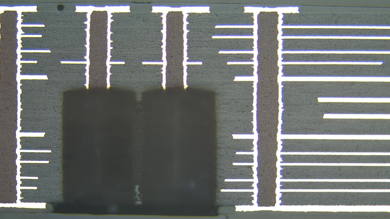
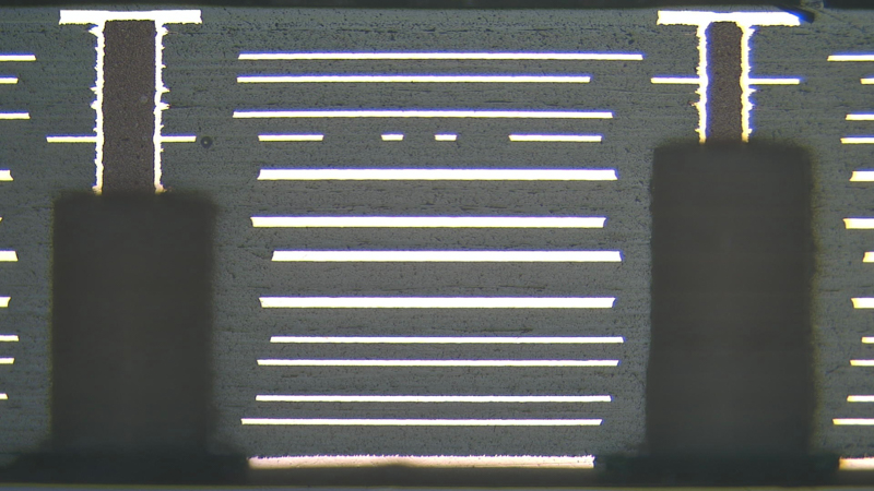

Design considerations for using this technology in your printed circuit boards:
- Use a back drill chart: Back drill charts help designers determine the optimal drill diameter and depth for each signal layer. This can prevent back-drilling errors that can lead to signal degradation and signal loss.
- Choose the right back-drilling process: There are different back-drilling processes available, such as laser ablation, mechanical drilling, and plasma etching. Each process has its own advantages and disadvantages, so designers should choose the process that best suits their board design.
- Avoid back drilling vias that are too close to the edge of the board: Back drilling vias that are too close to the edge of the board can cause problems during the drilling process, such as drill bit breakage or board damage.
- Use controlled impedance routing: Controlled impedance routing can help prevent signal reflections and ensure signal integrity. This is especially important for high-speed signal lines that are back-drilled.
- Minimize the number of back-drilled vias: Back drilling can be a time-consuming and expensive process, so designers should try to minimize the number of back-drilled vias. This can be achieved by carefully selecting the layer stack-up and using blind and buried vias.
Specialized Equipment
Not every PCB shop may offer back drilling as a service as it requires specialized equipment and expertise, so it's possible that some shops may not have the capability or experience to provide this service.
To perform back drilling, a PCB shop will need specialized drilling equipment and software that can precisely control the depth and diameter of the holes being drilled.
Key pieces of equipment needed for back drilling:
- CNC Drilling Machine: A CNC drilling machine is used to drill the holes in a PCB with precision and accuracy. For back drilling, the machine needs to have the ability to control the depth of the drill bit.
- Back Drilling Bits: Special back drilling bits are used to remove the unwanted copper material from the drilled hole. These bits are designed to cut away the copper cleanly without damaging the surrounding copper.
- X-Ray Drilling Machine: An X-Ray drilling machine is used to verify the accuracy of the drilled holes. The X-ray system can check the depth of the hole to ensure that it matches the desired depth.
By taking all of these factors into consideration and working with an experienced PCB fabricator, the PCB designer can ensure that their circuit board is back-drilled efficiently and effectively, resulting in improved signal integrity.

